16th USENIX Security Symposium
Pp. 291–306 of the Proceedings


Active Hardware Metering for Intellectual Property
Protection and Security
Yousra M. Alkabani
Computer Science Dept.
Rice University, Houston, TX
Farinaz Koushanfar
Electrical and Computer Engineering Dept.
Rice University, Houston, TX
We introduce the first active hardware metering scheme that aims to protect integrated circuits (IC) intellectual property (IP) against piracy and runtime tampering. The novel metering method simultaneously employs inherent unclonable variability in modern manufacturing technology, and functionality preserving alternations of the structural IC specifications. Active metering works by enabling the designers to lock each IC and to remotely disable it. The objectives are realized by adding new states and transitions to the original finite state machine (FSM) to create boosted finite state machines(BFSM) of the pertinent design. A unique and unpredictable ID generated by an IC is utilized to place an BFSM into the power-up state upon activation. The designer, knowing the transition table, is the only one who can generate input sequences required to bring the BFSM into the functional initial (reset) state. To facilitate remote disabling of ICs, black hole states are integrated within the BFSM.
We introduce nine types of potential attacks against the proposed active metering method. We further describe a number of countermeasures that must be taken to preserve the security of active metering against the potential attacks. The implementation details of the method with the objectives of being low-overhead, unclonable, obfuscated, stable, while having a diverse set of keys is presented. The active metering method was implemented, synthesized and mapped on the standard benchmark circuits. Experimental evaluations illustrate that the method has a low-overhead in terms of power, delay, and area, while it is extremely resilient against the considered attacks.
In the dominant horizontal semiconductor business model, piracy (illegal copying) and tampering of hardware are omnipresent. In the horizontal business model, hardware IPIn this paper, the term IP is used to refer to the integrated circuits design specifications that is available to the fabrication house. designed by the leading edge designers are mostly manufactured in untrusted offshore countries with lower labor and operational cost. This places the designers in an unusual asymmetric relationship: the designed IP is transparent to the manufacturers, but the fabrication process, quantity and added circuitry to the manufactured integrated circuits (ICs) by the foundry are clandestine to the designers and IP providers.
The security threat, financial loss and economic impacts of hardware piracy which have received far less attention compared to software, is even more dramatic than software [31,8]. Software piracy has received more attention compared to hardware also because it requires low-cost resources that are available to the general public. Protection of hardware is also crucially important because the ICs are pervasively used in almost all electronic devices and the potentially adversarial fabrication house has the full control over the hardware resources being manufactured. It is estimated that the computer hardware, computer peripherals, and embedded systems are the dominant pirated IP components [31].
Several other issues make the IC protection problems truly challenging: (i) very little is known about the current and potential IC tampering attacks; (ii) numerous attacking strategies exist, since tampering can be conducted at many levels of abstraction of the synthesis process; (iii) the most likely hardware adversaries are financially strong foundries and foreign governments with large economic resources and technological expertise; (iv) the adversary has full access to the structural specification of the design and most often also to the manufacturing test vectors; (v) the internal part of manufactured ICs are intrinsically opaque. While it is possible to tomographically scan an IC, the dense metal interconnect in 8 or more layers of modern manufacturing technology greatly reduce the effectiveness of such expensive inspections.
IC metering is a set of security protocols that enable the design house to gain post-fabrication control by passive or active count of the produced ICs, their properties and use, or by remote runtime disabling.
Our strategic goal is the development, implementation, and quantitative evaluation of symmetric mechanisms and protocols for hardware protection procured by untrusted synthesis, manufacturing, and/or testing facilities. The term symmetric emphasizes that both the designers and the foundry will be protected by the new methods. The symmetry is warranted by the unique variabilities and the key exchange mechanism that is based on the agreement of both parties for unlocking each IC.
Hardware metering is important from both commercial and military point of views. For example, without metering, a foundry can produce numerous copies of one design without paying royalties, or, as another example, the sensitive defense designs may become available to adversaries. The passive hardware metering schemes work by giving a unique ID to each chip [20,17,21]. The first ever active hardware metering method introduced in this paper, provides not just mechanisms for detection of illegal copies, but more importantly, ensures that no manufactured IC can be used without the explicit consent of the designer.
The proposed methods employ two generic security mechanisms: (1) uniqueness of each IC due to manufacturing variability; and (2) structural manipulation of the design specification while preserving behavioral specification. While the first mechanism has been already proposed and used for unique IC identification, the second is novel. Even more novel is the integration of two mechanisms, a task that requires a great deal of creativity and formation of solutions to a spectrum of challenging technology, synthesis and optimization problems, with a greater impact than the sum of the powers of the individual techniques.
The integration to the functionality is performed by interwinding the unique unclonable IDs for each chip into the FSM of the design. The integrated control part is denoted by BFSM, and is built by adding new states and transitions to the original FSM, while preserving the original functionality of the circuit. To bring the BFSM into the functional initial (reset) state, knowledge of the transition table is required. Since the designer is the only one who knows this information, no one else can generate a key with a finite amount of resources to unlock the IC. Using a combination of BFSM and newly added black hole states, remote disabling of the ICs can be made possible. We outline several possible attacks against the introduced active hardware metering method and provide mechanisms that neutralize the impact of those attacks. For example, we show how addition of the black hole states disable the random guessing attacks.
The remainder of the paper is as follows. After describing the background, flow and the state-of-the-art in the next two sections, we represent the active metering method in Section 4. In Section 5, we show a low-overhead implementation and obfuscation of active metering. Section 6 introduces potential attacks and the countermeasures that needs to be taken to be resilient against the attacks. We present experimental evaluation of the prototype implementation on several standard design benchmarks in Section 7. We outline a number of potential applications in Section 8 and conclude in Section 9.
2 Preliminaries
In this section, we describe the necessary background required for understanding the active hardware metering approach. The aim is to make the paper self-contained for the readers who are not familiar with the hardware design and synthesis process. Next, we describe the global flow of the active hardware metering approach.
Manufacturing variability (MV). The intense industrial miniaturization of CMOS devices has been driven by the quest for increasing computational speed and device density, while lowering cost-per-function, as predicted by Moore's law. CMOS variations result in high variability in the delay and the currents of the VLSI circuits. The variations might be temporal or spatial. The temporal variations may occur across nanoseconds to years [24]. Spatial variation is due to lateral and vertical differences from intended polygon dimensions and film thicknesses . Spatial variation may be intra-die, or inter-die [27]. Aside from device variations, the circuit response and its variability are correlated with circuit topology. We will utilize the spatial variations in our benefit, while we address the problem of alleviating temporal variability. Bernstein et al. provide a classification of device variations (beyond 65nm) [4].
Design descriptions. We consider the case in which the sequential design in question represents a fully synchronous flow and that the description of its functionality from an input/output (I/O) perspective is publicly available. We assume that the functionality is fully fixed, in that the I/O behavior is fully specified. Therefore, we utilize unique unclonable identification to embed a distinct mark in the functionality of each IC, without altering the functionality in terms of the normal I/O behavior of the circuit. Our technique is applicable to the case where the piece of IP is available in structural HDL description, or in form of a netlist that may or may not be technology dependent. The description uniquely defines the sequential circuit's behavior and the state transition graph (see the next subsection) of the design.
During the design flow, the user will take such a description and if required, will map it to a specific technology. Typically, logic level optimizations such as retiming are performed at this stage. Most often, the circuit is used as a part of a more complex design.
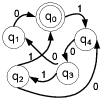 Figure 1: Figure 1:
Example of a STG with five states.The inputs required for state-to-state transition are shown next to the edges.
Finite state machine (FSM). FSM is a discrete dynamical structure that translates sequences of input vectors into sequences of output vectors. FSM can represent any regular sequential function. It appears in different forms, e.g. case statements in VHDL and Verilog HDL. The FSM is defined by the tuple  =(
=( ,
, ,
, ,
, ,
, ,
, ), where
 and
and
 are a finite set of inputs and outputs symbols respectively;
={
,
are a finite set of inputs and outputs symbols respectively;
={
, ,
, }
} 0 is a finite set of states while
is the "reset" state; and the transition function is denoted as
0 is a finite set of states while
is the "reset" state; and the transition function is denoted as
 on the input
  and the set

 , while the output function is denoted as
on the set
, while the output function is denoted as
on the set
 .
.
To represent the state transitions and output functions of the FSM, we use the state transition graph (STG), with nodes corresponding to states and edges defining the input/output conditions for a state-to-state transition. An example STG is shown in Figure 1, where there are five states {
,
,  ,
,  ,
,  },
is the reset state, and there is a one-bit input controlling the state-to-state transitions. In the remainder of the paper, we use the terms STG and FSM interchangeably to refer to the control part of the design.
},
is the reset state, and there is a one-bit input controlling the state-to-state transitions. In the remainder of the paper, we use the terms STG and FSM interchangeably to refer to the control part of the design.
As a motivational example for our problem, consider the scenario in which a given hardware intellectual property (IP) that belongs to its legitimate owner (Alice) is made available to a fabrication house (Bob). Alice pays for and demands  ICs implementing its design. Bob, utilizes the IP description to construct a mask that implements the design. Bob employs the mask to make
  copies of the design, where the illegal
  copies do not encounter much additional cost due to the availability of the mask. Bob may sell the
illegal copies and make a lot of profit with negligible additional overhead.
copies do not encounter much additional cost due to the availability of the mask. Bob may sell the
illegal copies and make a lot of profit with negligible additional overhead.
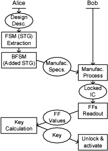 Figure 2:
The global flow of the active hardware metering approach.
The novel active metering helps Alice to protect her design against piracy by manipulating the STG of the original design, with the objective of creating a locked state, that is unique for each of the ICs manufactured from the design with a very high probability. Upon manufacturing by Bob, each device will be uniquely locked (i.e., rendered non-functional), unless Alice is contacted by Bob to provide the particular key to unlock the IC. The scheme gives the full control over the manufactured parts and operational devices from the IP to Alice.
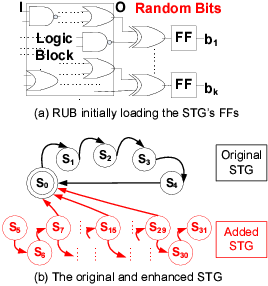
The global flow of the active hardware metering method is shown in Figure 2. We now describe the figure step by step. Alice takes the high level design description and synthesizes it to get the FSM of the design. Next, she constructs the BFSM by adding extra states. After that, she sends the detailed manufacturable design specifications to Bob who makes the mask and manufactures multiple ICs implementing the design. The manufactured ICs are locked (nonfunctional) at this stage. For each IC, Bob reads out the values in its flip flops (FFs) and sends the values to Alice. FF values can be read nondestructively, and the values are unique for each IC. Alice, knowing the BFSM structure, computes a specific key that can be used as input to that IC for unlocking it. The key is then sent back to Bob who utilizes it to activate the IC.
3 Related work
We survey the related literature that has influenced and inspired this work along four main lines of research: variability-based ID generation, authentication and security by variability-based IDs, intellectual property protection of VLSI designs, and invasive and noninvasive hardware attacks.
A number of authors have proposed and implemented the idea of addition of circuitry that exploits manufacturing variability to generate unique random sequence (ID) for each chip with the same mask [20,21,28]. The IDs are unclonable and separated from the functionality and do not provide a measure of trust, as they are easy to tamper and remove. Loftstrom et al. proposed a method for mismatching the devices based on changing the threshold of the circuits by placing the impurity of random dopant atoms [20]. Maeda et al. proposed implementing the random IDs on poly-crystalline silicon thin film transistors [21]. The drawback of the two described approaches is that they both need specialized process technology, and are easily detectable. Very recently, Su et al. have proposed a technique to generate random IDs by using the threshold mismatches of two NOR gates that are positively feeding back each other [28]. We will exploit their technique for the random ID generation.
A team of researchers has explored the idea of using variability-induced delays for authentication and security [9,19,29]. They use Physically Unclonable Functions (PUFs) that map a set of challenges to a set of responses, based on an intractably complex physical system. PUFs are unique, since process variations cause significant delay differences among ICs coming from the same mask. For each IC, a database of challenge-response sets is needed. Authentication occurs when the IC correctly finds the output of one or more challenge inputs. PUF-based methods solely utilize manufacturing variability as their security mechanism. In contrast, our proposed methods introduce a paradigm shift in hardware security by adding new strong mechanisms: integration into circuit functionality at the behavioral synthesis level. Further more, even though the active metering methods can be utilized for authentication, its main target is addressing the hardware piracy problem.
Koushanfar et al. have introduced the first hardware metering scheme that gives unique IDs to each IC [16]. The scheme was to make a small part of the design programmable so that one could upload different control paths post fabrication. They further described how to generate numerous different instances of the same control path with the same hardware [17]. They have also provided probabilistic proofs for the number of identical copies and probability of fraud for the proposed metering schemes [16,17]. All metering schemes were passive. Indeed, no active metering scheme has been proposed to date. The prior work in trusted IC domain also includes introduction of several watermarking schemes that integrate watermarks to the functionality of the design at the behavioral synthesis level [12,11,30,22,23,13,32,15]. Watermarking is a fundamentally different problem when compared to metering. It addresses the problem of uniquely identifying each IP and not identifying each IC, so the existence of the same mask does not affect the watermarking results. Fingerprinting for unique identification of programmable platforms has been proposed [18], but the techniques are not applicable to application specific designs (ASICs) due to the existence of a unique mask. Qu and Potkonjak provide a comprehensive survey of the watermarking, fingerprinting and other hardware intellectual property protection methods [23].
Even though many strong cryptographical techniques are available in hardware and software, their attack resiliency has been only verified by classical crypto-analysis methods. A class of attacks that is very challenging to address consists of physical techniques. Physical attacks take advantage of implementation-specific characteristics of cryptographical devices to recover the secret parameters. Koeune and Standaert provide a tutorial on physical security and side-channel effects [14]. The physical attacks are divided into invasive and noninvasive [3]. Invasive attacks depackage the chip to get direct access to its inside, e.g., probing. Noninvasive attacks rely on outside measurements, e.g., from the pins or by X-raying the chip, without physically tampering it.
There are multiple ways to attack an IC, including probing, fault injection, timing, power analysis, and electromagnetic analysis. Invasive attacks are typically more expensive than the noninvasive ones, since they need individual probing of each IC. Note that, according to the well-established taxonomy of physical attacks, attacks by the funded organizations (e.g., foundries) are the most severe ones, since they have both the funding and technology resources [1,2,3].
4 Active hardware metering
In this section, we present the details of the active hardware metering approach. Active metering is integrated into the standard synthesis flow, and is low overhead, generalizable, and resilient against attacks. By generalizable, we mean that the lock can be implemented on structures that are common to all designs. By attack-resiliency, we mean the cryptographic notion of a lock: that an attacker that does not have infinite computational power should not be able to unlock the IC without the knowledge of a key. To be generalizable, the method proposed here aims at protecting the design by boosting the design's FSM (and creating a BFSM) common to the widely used class of sequential designs. In this section, we describe the BFSM construction and introduce the locking mechanism. Implementation details are discussed in the next section.
Random Unique Block (RUB). Perhaps the most important component of the proposed security mechanism is the existence of the unclonable unique ID for each IC. The IDs are a function of the variability present at each chip and are therefore, specific to the chip. RUB is a small circuitry added to the design, whose function is to generate the unique ID. It is desirable that the RUBs do not change and remain stable over time. Recently, a few paradigms for designing unique identification circuitry was proposed [20,21,28]. The resulting IDs are mostly stable, and we will later show how to extract a nonvolatile ID from the RUB, even in presence of a few unstable bits.
Addition of the BFSM. The key idea underlying the proposed active metering scheme can be described in a simple way. Assume that the original design contains  distinct states. Further assume that the state of STG are stored in
  , 1-bit flip flops (FF�s). The FF�s represent a total of 2
 states, out of which
states correspond to the original design and (
states, out of which
states correspond to the original design and ( ) states are don�t cares. The metering mechanism adds an extra part to the FSM of the design. The added states are devised such that there are a number of transitions from the states in the added STG to the reset state
of the original design.
) states are don�t cares. The metering mechanism adds an extra part to the FSM of the design. The added states are devised such that there are a number of transitions from the states in the added STG to the reset state
of the original design.
In our scheme, the power-up state of each IC is built to be a function of the manufacturing variability and thus, will be unique to each instance. Furthermore, we select
such that
 . This selection ensures that when the circuit is powered up, its initial state will be in one of the added states in BFSM. Assume that the IC is powered up in the added state
  . During the standard testing phase, the manufacturer can read the state of the design, e.g., by scanning and reading the FF's. However, unless the foundry has the knowledge of the STG, finding the sequence of inputs required for the correct transition from the state
to the reset state
is a problem of exponential complexity. Essentially, there will be no way of finding the sequence other than trying all the possible combinations.
. During the standard testing phase, the manufacturer can read the state of the design, e.g., by scanning and reading the FF's. However, unless the foundry has the knowledge of the STG, finding the sequence of inputs required for the correct transition from the state
to the reset state
is a problem of exponential complexity. Essentially, there will be no way of finding the sequence other than trying all the possible combinations.
More formally, assume that the sequence of  primary inputs denoted as
  ={
={ ,
,  ,
,
,
,  } applied to the state
is one correct sequence of states that starts from
traverses
states denoted by
} applied to the state
is one correct sequence of states that starts from
traverses
states denoted by  ={
={ ,
,  ,
,
,
,
 ,
}, i.e.,
=
,
}, i.e.,
=
 . Assuming that the input is
  bits and there are cycles in STG, finding the correct input sequence that would result in
consecutive correct transitions is a problem with exponential complexity with respect to
and is thus, intractable.
bits and there are cycles in STG, finding the correct input sequence that would result in
consecutive correct transitions is a problem with exponential complexity with respect to
and is thus, intractable.
As an example, consider the STG shown in Figure 3(b) that consists of the original STG that has five states ({
,
,
,
,
}) with augmentation of twenty seven added states ({ ,
, ,
,
,
, }). Edges are incorporated to the added states to ensure that there are paths from each of the added states to the reset state of the design. The block shown in Figure 3(a) is a RUB.
Figure 3:
The boosted FSM (BFSM).
|
|
The output of the RUB defines
random bits that will be loaded into the FF's of the augmented STG upon start-up. Now, an uninformed user who does not have the information about the transition table (e.g., foundry), can readout the data about the initial added state
, but this information is not sufficient for finding the sequence of primary input combinations to arrive at the reset state
. However, the person who has the information about the structure of the STG, upon receiving the correct state, would exactly know how to traverse from this locked state to
. In other words, the owner of the FSM description is the only entity who would have the key to unlock the IC.
An interesting application of the proposed BFSM construction method is in remote disabling. Alice will save the RUBs and the keys for all the ICs that she has unlocked. Using the chip IDs that are integrated within the functionality, she can add mechanisms that enable her to monitor the activities of the registered chips remotely, for example, if they are connected to the Internet. She can further add transitions from the original STG to untraversed states, to lock the IC in case it is needed. Remote disabling has a lot of applications. For example, it can be used for selective remote programming of the devices, and royalty enforcement.
4.2 Ensuring proper operation
The following issues and observations ensure proper operation and low-overhead of active hw metering:
(i) Storing the input sequence (key) for traversal to the initial state
. During testing, once Bob scans out the FF values and sends them to Alice, she provides the key to Bob. He includes both the original RUB and the key in the chip, for example, in a nonvolatile memory. This data is utilized along with the unclonable RUB circuit, for transition to the reset state. Since the power-up state is unique for each IC, sequence of inputs (key) that traverse the power-up state to the reset state is also specific to each IC. One needs to store the key which performs the traversal at the power-up state on each chip. There are many ways to accomplish this. For example, the designer could add a small programmable part to the design which needs to be coded with the unique sequence (key) before each IC is in operation. Coding ensures protection of keys against other software attacks. As an alternative, the sequence might not be included in the memory and just used as a permanent password to the IC.
(ii) Powering up in one of the added states. This condition can be easily guaranteed by selecting a large enough
. Assuming that all the states have an equal probability, the probability of starting in one of the added states is (
)/ . For a given
, we select
such that the probability of not being in one of the added states is smaller than a given probability. For example, for
. For a given
, we select
such that the probability of not being in one of the added states is smaller than a given probability. For example, for  and
and  , the probability of starting up in an original state is less than
  .
.
(iii) Diversity of power-up states (unique IDs).
should also be selected so that the probability of two ICs having the same ID becomes very low. Assume that we need to have  distinct ICs each with a unique ID. Assuming that the IDs are completely random and independent, we utilize the Birthday paradox to calculate this probability and to make it low. Consider the probability
 that no two ICs out of a group of
will have matching IDs out of
equally possible IDs. Start with an arbitrary chip's ID. The probability that the second chip's ID is different is (
that no two ICs out of a group of
will have matching IDs out of
equally possible IDs. Start with an arbitrary chip's ID. The probability that the second chip's ID is different is ( )/
. Similarly, the probability that the third IC's ID is different from the first two is [(
)/
].[
)/
. Similarly, the probability that the third IC's ID is different from the first two is [(
)/
].[ /
]. The same computation can be extended through the
-th ID. More formally,
/
]. The same computation can be extended through the
-th ID. More formally,
Thus, knowing
, the number of required distinct copies, and setting a low value for  , we would be able to find
that satisfies the above equation.
, we would be able to find
that satisfies the above equation.
(iv) Overhead of the added STG. The number of states increases exponentially with adding each new bit, and thus, the scheme has a very low overhead. Note that, in modern designs, the control path of the design (i.e., FSM) is less than 1% of the total area and hence, adding a small overhead to the FSM does not significantly affect the total area [7,10]. In the next section, we will describe a low-overhead implementation of the proposed method.
(v) Diversity of keys. There is a need to ensure that the keys are distinct in all parts of their sequences, or there is a very small shared subsequence between different keys. This is granted by making multiple paths on the graph from each of the states to the reset state. We will elaborate more on this issue in the attack resiliency section.
5 Low overhead implementation and obfuscation
In this section, we discuss the implementation details of the RUB and the BFSM that are the required building blocks for the active hardware metering approach. We start by outlining the desired properties of each block, and then we delve into its implementation details.
A critical aspect of the proposed security and protection mechanisms is the generation of random ID bits. There are a number of properties that the RUB implementation has to satisfy, including:
 Low overhead. The added parts must not introduce a significant additional overhead in terms of delay, power consumption and the area.
Distribution of IDs and their correlations. To have the maximal difference between any two ID numbers (the maximal Hamming distances) the ID bits must be completely random. Thus, no correlation must be present among the ID bits on the same die or across various dies.
Indiscernibility. The IDs must be integrated within the design, such that they cannot be discerned by studying the layout of the circuit. For example, the IDs should not be placed in a memory-like array, where the regularity of the array and its connections to the FFs could be easily detected.
Stability. There is a need to stabilize the IDs over the lifetime of an IC. This is particularly important since studies have shown the temporal changes in CMOS process variations due to many environmental and aging effects including, residual charges, self-heating, negative-bias temperature instability, and hot electron effects [4].
For implementing the random IDs, we employed the recent novel approach proposed by Su et al. [28]. They have designed and tested a new CMOS random ID generation circuit that relies on digital latch threshold offset voltages. Using cross coupling of gates, they report significant improvement in readout speed and power consumption over the existing designs.
Each ID bit is generated by cross-coupled NOR gates. The latch sides are pulled low initially. At the high to low clock transition, the state of each latch is determined by the threshold voltage mismatch of the transistors. Essentially, the approach relies on the positive feedback inherent in the latch configuration to amplify the mismatch. This design removes the need for comparators, low offset amplifiers, or extra dopants needed in previous random ID generation methods [20,9]. The nominal overhead of the above proposed approach is two NOR gates per bit. The authors have reported 96% stable IDs using this method, while using dummy latches to protect the IDs.
Even though we use the random bit architecture described above, our layout and implementation of random bits are very different. To be indiscernible, we do not place the coupled NOR gates in an array, and instead synthesize them with the rest of the circuit and camouflage them within the sea of gates. based on invariability of the ID bits for an IC. In Subsection 6.2, we provide a mechanism that ensures the occasional errors in ID bits do not affect the hardware metering approach.
The key design objectives and challenges of the BFSM are as follows:
Low overhead. The addition of the states to the original FSM must have a low overhead in terms of area, power, and delay. This is particularly challenging: as we have computed in Subsection 4.2, even under the assumption of having RUBs with Uniform distribution of random bits, the number of added states must be exponentially high to ensure a proper operation.
Traversal path. There must be a path on the BFSM, from each of the power-up states (except for the black hole states that we will describe in Section 6.2) to the reset state.
States obfuscation. The states must be completely obfuscated and interchanged to camouflage the added STG and the original STG. Another level of obfuscation is disabling the observability of the FFs, so that similar states on two ICs do not exactly have the same code scanned out from their FFs.
Multiplicity of keys. It is highly desirable to construct the paths on the added STG in such a way that there are multiple paths from each power-up state to the reset state. This will ensure that there are multiple keys for traversal. Now, if the states are obfuscated such that a similar state on two ICs has different codes, and each of them gets a different key for traversal to the original STG, the state similarities will not be apparent, even to a smart observer.
To achieve a low overhead, we have systematically designed STG blocks that are capable of producing an exponential number of states with respect to their underlying hardware resources. The blocks are designed such that there are multiple paths from each of the added states to the reset state and thus, the multiplicity of the keys is satisfied. Our first attempt was to synthesize the added blocks of STG and the original STG together. However, because the synthesis software automatically optimizes the interwoven architecture, it most often ended up with a combined STG that was much larger than the sum of its components. Thus, we decided to first separately synthesize the original and the added STG before we merge them. Next, we employed obfuscation methods that constantly alter the values of the FFs, even those that are not used in state assignment in the current STG. As we will see in attack resiliency section, the introduced obfuscation method has the side-benefit that the adversary cannot exactly distinguish a similar state on two different ICs.
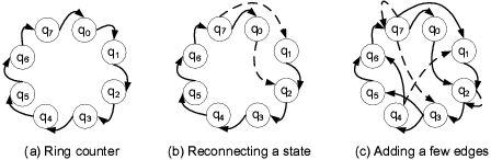
The added STG can be designed to be low overhead; there are exponentially many states for each added FF, ignoring the overhead of the STG edges. However, in real situations, the transitions (edges) require logic. Thus, the added STG is constrained to be sparse to satisfy a low overhead. We have built this block in a modular way. We describe one of our modules here and then discuss systematically interconnecting the modules to have a multi-bit added STG that has a low overhead.
Figure 4:
Illustration of steps for building a sparse 3-bit STG.
|
The first module is a 3-bit added STG. In Figure 4, we show three steps for building this module. We start by a ring counter as shown in Graph 4(a). Next, we pick a few states and reconnect them to break the regularity. A small example is illustrated in Graph 4(b), where the state
is reconnected, such that still there will be a path from each state to any other state. Finally, we add a few transitions (edges) to the STG, like the example shown in Graph 4(c); here the states
and
are reconnected, while the edges {
 ,
,
 ,
,
 ,
,
 } are added.
The example is just an illustration. Many other configurations are possible. The various combinations have different post-synthesis overhead. To ensure a low-overhead, we exhaustively searched the synthesized 3-bit structure with various sparse edge configurations like the example above, and selected the configurations with the lowest overhead as our 3-bit modules. As it is apparent from the structure, many low-overhead configurations are possible and we do not need to use the same module multiple times.
After that, we picked the low overhead modules and started to add edges to interconnect them, such that the connectivity property is satisfied, and the interconnected configuration still has low overhead. Furthermore, we need multiple interconnecting paths that can produce multiple keys. This is again done via a modular randomized edge addition and searching the space of the synthesized circuits to find the best multi-bit configurations. Note that, the synthesis program performs state-encoding for the interconnected modules. We have noticed that the distance of the codes assigned to the states does not have a correlation with the proximity of the states. Therefore, even for two RUBs that are only different in 1-bit, typically the power-up states are not close-by on the added STG.
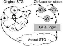
In our experiment, we have tested our approach on 12, 15, and 18-bit added STGs. Now, the original STG has to be glued to the added part. This is done by an obfuscation scheme that ensures the states of FFs that are associated with the original STG keep pseudorandomly changing, even when we traverse the states of the added STGs. Thus, for an observer who studies the values of the interleaved FFs, the activity study would not yield an informative conclusion that can help separating the original and the added states. A simple example for this obfuscation is depicted in Figure 5. In this figure, a small original STG with five states is presented. The cloud shown below the original STG indicates the added states.
Figure 5:
Obfuscation of the original STG.
|
|
There are multiple state transitions from the added states to the original state. However, we only show one arrow on the plot not to make it more crowded. In this example, we use the three don't cares of the design for obfuscation purposes. There are 3 don't care states that we use to form three new dummy states  ,
,  , and
, and  , illustrated in grey color. The glue logic attaches the inputs and the states of the added STG to the dummy STG. Thus, by carefully designing, one can alter the bits on the dummy STG by changing the input and the states of the added STG without touching the original FSM. If the design does not have sufficient don't cares, we can add a couple of FFs for the dummy states and use the same paradigm. The important requirement for the dummy states is that as a group they should present both 1 and 0 digits in all FFs. The original STG is also connected to the dummy STG and can utilize it as a black hole (described more thoroughly in Subsection 6.2), if there is a need to halt the IC.
6 Attack resiliency
This section first identifies several types of potential attacks on the active hardware metering approach. Next, we outline a number of mechanisms that must be added to the basic active metering scheme to ensure its resiliency against the suggested attacks.
The adversary (Bob) may attempt to perform a set of invasive or noninvasive attacks on the proposed active metering scheme. Bob may do so by measuring and probing one instance, or by statistically studying a collection of instances. In this section, we first identify and describe the attacks. Next, we propose efficient countermeasures that can be taken to neutralize the effect of potential adversarial acts.
We assume that Bob knows all the concepts of the proposed hardware metering scheme, has the complete knowledge of the design at all levels of abstraction provided to the foundry (e.g., logic synthesis level netlist, and physical design GDS-II file, but no behavioral specification), can simultaneously observe all signals (data) on all interconnects and flip-flops (FFs), and can measure, with no error, all timing characteristics of all gates in the ICs.
The starting point for development and evaluation of the metering schemes is identification and specification of several types of potential attacks:
(i) Brute-force attack. Bob aims to place the pertinent IC into the initial state by systematically applying the input sequences to the BFSM. The systematic application may be a randomized strategy, or may be based on scanning the FFs. Brute-force attack works by randomly changing the inputs in hope of arriving at the reset state. Scanning works by reading out the FF values for a few ICs and storing them. The FFs in the current IC are then monitored for the existence of a common state with the stored ones. In case a state that was read in the previous ICs is reached, Bob uses the same key for traversal to the reset state.
(ii) Reverse engineering of FSM. Bob may try to scan the FFs to extract the STG. The attempt would be to remove the added STG from the BFSM, to separate the original and the added states.
(iii) Combinational redundancy removal. Bob may use the combinational redundancy removal, a procedure that attempts to remove the combinational logic that is not necessary for the correct behavior of the circuit. The proposed techniques of this class often take into account the set of reachable states of the FSM under examination [25]. Note that, the attacks that were described so far can greatly benefit from the ability to simultaneously monitor the multitude of signals/values on the IC using laser reading.
(iv) RUB emulation. The goal of this attack is to create a reconfigurable implementation capable of realizing hardware that has the identical functional and timing characteristics to a RUB for which a legal key is already received.
(v) Initial power-up state capturing and replaying (CAR). Bob knows the initial power-up state of an unlocked IC. He can use invasive methods to load the FFs of other ICs to the same power-up state as the unlocked IC and then utilize the same key to decode the new locks. Note that, unless invasive methods are used, the only way for Bob to alter the values in the FFs is to change the states using the input pins. Without the knowledge of the STG, the change of state can only be done as described in the first attack. This attack and the next two belong to the class of replay attacks.
(vi) Initial reset state CAR. Bob scans the FF of an unlocked IC and reads the code of the reset state. Next, he employs invasive methods to load the FFs of other ICs to unlock them.
(vii) Control signals CAR. In this attack, Bob attempts to bypass the FSM by learning the control signals and attempting to emulate them. Bob may completely bypass FSM by creating a new FSM that provides control signals to all functional units, and control logic (e.g. MUX's and FFs) in the datapath.
(viii) Creation of identical ICs using selective IC release. Bob only releases the ICs with similar characteristics to Alice in the hope of finding the keys by correlations. This attack is probably the most expensive because it involves only a small percentage of manufactured ICs by the untrusted foundry. Only the ICs that have similar RUBs are reported. Hence, if the attack is successful, the design house supplies many keys for ICs with similar RUBs; the birthday paradox shows that one of the keys with relatively high likelihood can be used on the unreported ICs. Note that, the way for Bob to determine closeness of characteristics is by looking at the distances of the initial power-up states.
(ix) Differential FF activity measurement. Bob may start to investigate the differential activities of the FFs of the unlocked designs for the same input, and then try to eliminate the FFs that have different values.
6.2 Countermeasures
We propose a number of mechanisms to augment the basic active metering scheme and preserve its security against the above attacks. Two important observations are that FSMs in modern industrial design are always a very small part the overall design, well below 1%, and that STG recovery is a computationally intractable problem [7,10,22]:
Figure 6:
Example of a black hole FSM.
|
|
Creating black holes FSMs. Alice may create a black holes FSM inside the BFSM that makes the exit impossible. Black holes are the states that cannot be exited regardless of the used input sequence. Their design is very simple as shown in Figure 6, where the black states do not have a route back to the other states. Furthermore, a designer can plan the black hole states to be permanent if it is desirable: a small part may be added, so that restarting the IC would not take it out of the black hole states. This measure essentially eliminates the effectiveness of the first two attacks, because no random input sequence leads to the initial state of the functional FSM: once the black hole sub-FSM is entered, there is no way out. A special case is creation of trapdoor black (gray) holes FSMs that are designed in such a way that only long specific sequence of input signals known just to the designer can bring control out of this FSM and into the initial functional state of the overall FSM. An issue that needs to be carefully addressed here is preventing the IC from powering-up in one of the black-hole states. This can be easily ensured by adding extra logic to the black hole parts that would disconnect the black hole states from the power-up states.
Merging the functional BFSM with the test and other FSMs, (e.g. ones that can be used for debugging and authentication). In a typical design, the functional control circuits are not the only FSMs around. Alice, with the the objective to make identification of her functional FSM more difficult, can further intricate the BFSM by co-synthesizing them with others. This augmentation makes the first two and the three CAR attacks less effective. In particular, this merger would distract the ability to simultaneously monitor the multitude of signals/values on the IC using laser reading.
Similar FF activity for the unlocked ICs. The designs would be made such that once an IC exits the locked states and is in its functional states, all its FFs have a deterministic behavior that is the same for all ICs. Thus, the differential FF activity screening would not yield any useful information.
Creation of specialized functional FSMs (SFFSMs). Alice can make the security much tighter by integrating the RUBs not just to assign the initial power-up state, but to alter the structure of the BFSM and make it a SFFSM. Using this method, the reset state for FSM of each IC is a function of its RUB. Each SFFSM operates correctly only if it received a specific stream of signals from the RUBs. Since there are exponentially many states with respect to the number of FFs in FSM, we map a set of blocks that share an identical subset of RUB outputs into a single SFFSM. This countermeasure makes the first two attacks (i.e., brute-force attack and FSM reverse engineering) much more difficult and the first two CAR attacks (i.e., initial control signal CAR and initial reset state CAR) almost impossible.
A simple example of this method is presented in Figure 7. On this figure, the added STG is shown by the cloud on left, and the original STG is plotted in the right cloud. The original STG has only 3 states: a reset state two other states. Here, the original STG is replicated twice: One replication is denoted by SFFSM' and the other one is denoted by SFFSM". The scheme adds logic to the added STG, so based on the bits in the RUB, it will be categorized into three classes. Each of the classes will transition to one of the reset states in one of the clouds: original FSM, SFFSM' or SFFSM". This scheme will cause confusion in FFs scanning methods that aim at loading the reset state of an unlocked IC in the FFs of a locked chip. Note that, the replicated states need not all be unique, and maybe shared among the replicas to reduce the overhead.
Figure 7:
A simplified SFFSM.
|
|
The example is very small, but one can add the RUB-dependent states at various stages to ensure that the attacker is not able to break the system. A combination of the SFFSM method and the state obfuscation and encoding would ensure a full security of the design against the CAR attacks. Furthermore, using similar methods, the RUBs can be also added to the obfuscation scheme based on the dummy variables like the example presented in Figure 5, so that the same inputs would have different random obfuscation patterns.
Another use of SFFSM is for addressing the effect of temporal changes in RUB. Recall that the actual application of the new hardware metering scheme to industrial designs requires mechanisms that ensure resiliency against time-dependent permanent changes of transistors as well as gate-level and transient changes due to the environmental conditions such as temperature and supply voltage fluctuations [4].
The exact reconstruction of the first power-up state of IC (the particular one for which the designer released the key) for the purpose of defeating the variabilities is trivial: Bob can just load the captured and saved outputs of the first power-up RUB for which he has obtained the key. This mechanism makes the design susceptible to reuse attacks, where Bob can reuse the key and the initial RUB for an unlocked IC to decipher another locked IC. However, if Alice included SFFSM in her design, she would be resilient against this attack. The only technical issue that remains to be addressed is to ensure that the SFFSM receives the correct data from the physical RUB, exactly the same as the one that was first received and for which the key is available. Otherwise, the stored key will fail.
In presence of temporal variations, ensuring that each SFFSM receives the correct data from RUB requires error-correction mechanisms. One solution is to employ standard error-correction codes (ECCs). An alternative hardware solution that encounters a lower overhead compared to ECC is to create the specifications of each SFFSM in such a way that it transitions into the correct next states, even when one or up to a specified number of the inputs from the RUB are altered by the environmental conditions. Using the hamming distances of the RUBs, we can group them into similar SFFSMs and synthesize the results such that the error correction mechanisms are inherently present. This mechanism is particularly effective for longer RUBs that are required for present industrial designs. Note that, because the minterms for the combinational logic that implements transitions are now not smaller than for non-resilient versions of the SFFSM, the hardware overhead is often zero or negative at the expense of the lower resiliency against brute force attacks [5]. However, since the probability of brute force attack can be made arbitrarily small with very low overhead (i.e., by using the black holes), this is a favorable trade-off.
Resiliency against combinational redundancy removal. To overcome this attack, Alice must ensure the inapplicability of the attack to typical large circuits and the capability of this method to remove the added states. In general, computing a set of reachable states, can only be done for relatively small circuits, even when the implicit enumeration techniques are used. Thus, the method is only applicable to small circuits of small sizes.
Statistical characterization of gates. Alice can go one step further and attempt to derive the gate-level characteristics of the manufactured ICs by measuring the input/output signals and exploiting the controllability and observability into the design. Essentially, knowing the circuit diagram, she would be able to write a linear systems of equations that can be solved for obtaining the approximate gate-level delay and power characteristics of the gates. She may even go further to use the extracted data to find the distribution of variations across the different chips (e.g., by using methods such as expectation maximization(EM)). Now, if the variations do not have enough fluctuations, then she will get suspicious and can halt the unlocking. This computation would ensure that the selective IC release would not be successful.
Obfuscation of state activities and encodings. The implementation of the BFSM presented in the previous section renders it impossible to tell the difference between the original FSM FFs and the added states FFs. This is because all of the FFs are changing all the time. Therefore, even though two states of BFSM in two ICs might be identical, the attacks based on scanning the FFs would not notice that, since a subset of the bits will be different. In other word, the FFs not used in the added FSM are randomly changing. Another obfuscation method that has already been implemented is that the states in the added STG are not in order and are coded out of sequence by the synthesis tool. Thus, even though there might be a direct transition (edge) between two states, the methods based on FFs readings would not notice the proximity of the two states, since there code words are distant from each other.
Note that, the attacks that were described earlier, even the ones that are computationally very expensive, will not be able to unlock the ICs, if the countermeasures described above are in place.
7 Experimental evaluations
To test the applicability of the method described earlier, we implemented the active hardware metering on standard benchmark designs. In this section, we present the experimental setup, followed by the overhead of implementing BFSM on the considered benchmarks. After that, we show quantitative analysis of the effectiveness of the brute force attacks. We further show how the addition of black holes can make the scheme resilient against this attack with a minimal overhead. Note that, many of the attacks described earlier are assuming structural countermeasures that are hard to quantify and evaluate.
We used extended set of sequential benchmarks from the ISCAS'89 to evaluate the impact of the active hardware metering method [6]. Even though the ISCAS'89 benchmarks are the latest comprehensive set of the gate-level designs, they are dated compared to the complex circuits in design, production and use today. Recall that following the Moore's law, the size and complexity of the circuits doubles approximately every 18 months. We use the larger benchmarks from the set, and we project the results to more complex circuits. Our projections show that the power, area, and delay overheads diminish as we increase the size and complexity. Simultaneously, the locking complexity and resiliency against the attacks exponentially improves, due the multiplicity of states. We synthesize the benchmarks using the Berkeley SIS tool [26], that given a STG or a logic-level description of a sequential circuit produces an optimized netlist in the target technology (cell library) while preserving the sequential input-output behavior. We have written a C program that modifies the benchmarks by adding the extra states. The program calls SIS to obtain the specifications of the synthesized and mapped original and modified STGs. When evaluating the overhead results, the important observation is that FSMs (i.e., the control circuitry) in modern industrial design are always a very small part of the overall design, well bellow 1% [7,10]. Thus, even doubling the overhead, will have a minimal impact on the overall circuit that is mostly occupied by memory, testing pins, and data path circuitry.
Table 1:
Area overhead of active metering for various benchmarks.
| |
Original Details |
12 FFs |
15 FFs |
| Circuit |
In |
Out |
FFs |
Area |
Area |
% |
Area |
% |
|---|
| s27 |
4 |
1 |
3 |
18 |
224 |
11.44 |
278 |
14.44 |
| s298 |
3 |
6 |
14 |
244 |
454 |
0.86 |
508 |
1.08 |
| s344 |
9 |
11 |
15 |
269 |
480 |
0.78 |
534 |
0.99 |
| s444 |
3 |
6 |
21 |
352 |
554 |
0.57 |
609 |
0.73 |
| s526 |
3 |
6 |
21 |
445 |
648 |
0.46 |
702 |
0.58 |
| s641 |
35 |
23 |
17 |
539 |
743 |
0.38 |
797 |
0.48 |
| s713 |
35 |
23 |
17 |
591 |
793 |
0.34 |
847 |
0.43 |
| s953 |
16 |
23 |
29 |
743 |
947 |
0.27 |
1001 |
0.35 |
| s832 |
18 |
19 |
5 |
769 |
971 |
0.26 |
1025 |
0.33 |
| s1238 |
14 |
14 |
18 |
1041 |
1264 |
0.21 |
1318 |
0.27 |
| s1423 |
17 |
5 |
74 |
1164 |
1382 |
0.19 |
1436 |
0.23 |
| s9234 |
36 |
39 |
135 |
7971 |
8174 |
0.03 |
8228 |
0.03 |
| s13207 |
31 |
121 |
453 |
11248 |
11450 |
0.02 |
11504 |
0.02 |
| s38417 |
28 |
106 |
1463 |
32246 |
32448 |
0.01 |
32502 |
0.01 |
| |
|
|
|
|
|
|
|
|
|
Our first set of experiments study the overhead of the introduced scheme in terms of area, power, and delay. It is worth noting here that our ultimate goal is to integrate the active hardware metering method in the design flow. Thus we have considered testing the approach on manufactured ICs. However, the prohibitive cost of manufacturing a circuit in aggressive technologies (the quote we got for fabricating a circuit in 65nm was $500K) limits our experiments to synthesizing the benchmarks. Table 1 presents the results for the area overhead. Because of the relatively small size of the circuits, we added STGs with 12 FFs and 15 FFs overhead to the original STGs. The first column shows the name of the circuit from the ISCAS'89 benchmark. The second column shows the number of inputs to the circuit. The third column shows the number of outputs to the circuits. Both the number of inputs and the number of outputs do not change after adding the extra states. The fourth column shows the number of FFs in the original circuit. The fifth column shows the area of the original circuit. Then we show both the new area and the percentage overhead after adding 12 FFs and 15 FFs for the extra states. It can be seen that the percentage area overhead is decreasing as the circuit size increases. Thus, for larger circuit sizes, the area overhead will be even less insignificant.
Table 2:
Delay and power overhead of active metering for various benchmarks.
| |
Original Details |
12 FFs |
15 FFs |
| Circuit |
Delay |
Power |
Delay |
% |
Power |
% |
Delay |
% |
Power |
% |
|---|
| s27 |
6.60 |
134.00 |
14.40 |
1.18 |
1418.70 |
9.59 |
14.40 |
1.18 |
1696.70 |
11.66 |
| s298 |
15.00 |
1167.20 |
15.00 |
0.00 |
2468.60 |
1.11 |
15.00 |
0.00 |
2746.60 |
1.35 |
| s344 |
27.00 |
1030.00 |
27.00 |
0.00 |
2325.90 |
1.26 |
27.00 |
0.00 |
2603.90 |
1.53 |
| s444 |
17.60 |
1550.80 |
17.60 |
0.00 |
2815.20 |
0.82 |
17.60 |
0.00 |
3152.30 |
1.03 |
| s526 |
15.20 |
2065.70 |
15.20 |
0.00 |
3334.30 |
0.61 |
15.20 |
0.00 |
3664.70 |
0.77 |
| s641 |
97.60 |
1560.60 |
97.60 |
0.00 |
2832.10 |
0.81 |
97.60 |
0.00 |
3162.40 |
1.03 |
| s713 |
100.00 |
1670.70 |
100.00 |
0.00 |
2935.00 |
0.76 |
100.00 |
0.00 |
3265.40 |
0.95 |
| s953 |
23.60 |
1816.50 |
23.60 |
0.00 |
3084.20 |
0.70 |
23.60 |
0.00 |
3414.60 |
0.88 |
| s832 |
28.80 |
2849.60 |
28.80 |
0.00 |
4114.00 |
0.44 |
28.80 |
0.00 |
4444.40 |
0.56 |
| s1238 |
34.40 |
2709.40 |
34.40 |
0.00 |
4034.00 |
0.49 |
34.40 |
0.00 |
4312.00 |
0.59 |
| s1423 |
92.40 |
4882.70 |
92.40 |
0.00 |
6226.30 |
0.28 |
92.40 |
0.00 |
6504.30 |
0.33 |
| s5378 |
32.20 |
12459.40 |
32.20 |
0.00 |
13515.00 |
0.08 |
32.20 |
0.00 |
14057.50 |
0.13 |
| s9234 |
75.80 |
19385.50 |
75.80 |
0.00 |
20653.30 |
0.07 |
75.80 |
0.00 |
20983.70 |
0.08 |
| s13207 |
85.60 |
37874.00 |
85.60 |
0.00 |
39138.40 |
0.03 |
85.60 |
0.00 |
39402.00 |
0.04 |
| s38417 |
69.40 |
112706.80 |
69.40 |
0.00 |
113869.00 |
0.01 |
69.40 |
0.00 |
114147.00 |
0.01 |
| |
|
|
|
|
|
|
|
|
|
|
|
Table 2 shows the delay and power overheads. The first column contains the benchmark names. The second and third columns show the delay and power estimates of the original circuits. These are followed by both the delay and the percentage delay overhead, and the power and the percentage power overhead for adding both 12 FFs and 15 FFs STGs respectively. The delay overheads are universally small. With the exception of s27 that is too small to be considered practical, it is interesting to see that even other small benchmarks encountered no delay overhead after the addition of the new STG. For the small benchmarks that are not realistic compared to the current complex designs, the power increases significantly. As the circuit size increases, the percentage power overhead decreases.
Figure 8:
Percentage of (a) power; and (b) area; overheads vs. size after adding a1 5 FFs STG.
|
(a) % Power overhead vs. size.
|
|
(b) % Area overhead vs. size.
|
|
Next, we make a small model of the percentage of area and power overhead versus size of the circuit to extrapolate to more complex designs. The size of the added STG is fixed to 15 FFs. Figures 8(a) and 8(b) show the overhead data vs. size along with the fitted polynomial models, for power and area respectively. The plots suggest that as the circuit size increases, the percentage of power and area overheads both decrease. Note that, for more complex designs, it is required to add significantly more than 15 FFs. Even if adding a STG with 100 FFs would add six times the overhead of the 15 FFs case in absolute terms, the overhead would be negligible, while there will be  extra states added to the design. Thus, for current and future circuit technologies, the BFSM would have a minimal impact on the performance in terms of power, area, and delay (i.e., it will most likely stay less than 1% of the overall design).
Most of the attacks described in Section 6 can be encountered by devising intelligent design strategies, as described in Subsection 6.2. The only attack that we quantitatively study here is the brute force attack. We model this attack by randomly guessing the values on the graph until arriving at the functional reset state of the original FSM.
We simulated the brute force attack on BFSMs with 12, 15, and 18 FFs, varying the inputs from 3 to 8. In this experiment, we set an upper bound of 1,000,000 guesses; if the reset state is not reached after this many trials, the original STG is considered unreachable (denoted by N/R) and the brute force attack is reported unsuccessful.
Table 3:
Average number of attempts needed for the brute force attack to unlock the added STG.
| |
Number of inputs |
| bits |
3 |
4 |
5 |
6 |
7 |
8 |
|---|
| 12 |
74385 |
82708 |
78939 |
83156 |
77028 |
82490 |
|---|
| 15 |
560976 |
610373 |
602157 |
557776 |
592681 |
596260 |
|---|
| 18 |
933680 |
932501 |
938583 |
918312 |
N/R |
N/R |
|---|
| 12 + bh |
998000 |
999000 |
N/R |
N/R |
N/R |
N/R |
|---|
| 15 + bh |
N/R |
N/R |
N/R |
N/R |
N/R |
N/R |
|---|
| 12 + 2 bh |
N/R |
N/R |
N/R |
N/R |
N/R |
N/R |
|---|
| 12 + 2 bh |
N/R |
N/R |
N/R |
N/R |
N/R |
N/R |
|---|
|
Table 3 shows the average number of guesses needed to unlock the BFSM over a 10,000 simulation runs. The first three rows show added STGs with 12, 15, and 18 FFs respectively. The next two rows show the results for STGs with 12 and 15 FFs, after adding 1 and 2 black holes respectively. Although the number of inputs does not affect the overhead, it impacts the resiliency against the brute force attack: the table illustrates that the brute force attacks are less successful if we use more than 3 different inputs. Also, as the size of the added STG increases, more guesses are necessary to unlock the circuit. By adding one black hole to the smaller FSMs, they perform better than the larger FSMs. Adding one or two black holes makes the original STG unreachable for the brute force attack. It is worth noting here that STGs with 12 and 15 FFs are really small, as they have a total of 4,096 and 32,768 states respectively. If the active metering scheme was to be implemented on current industrial strength designs, the added circuit would have at least a 100 FFs that would create 2
 10
10 states. It would be impossible for a brute force attack to find a key. Furthermore, addition of a few black holes will further make the system resilient against the brute force attack.
Table 4 shows area and power overheads for adding a black hole with 2 states to added STGs with 12 and 15 FFs respectively. The overhead of adding a black hole does not exceed 5% even for very small benchmarks. For larger circuits it is unnoticeable. Note that, we often add more than one black hole to the design, to warrant the impossibility of the brute force attacks.
Table 4:
Percentage of area and power overheads after adding one blackhole.
| |
12 FFs |
15 FFs |
| Circuit |
% Area |
% Power |
% Area |
% Power |
| s27 |
0.05 |
0.04 |
0.04 |
0.03 |
| s298 |
0.02 |
0.02 |
0.02 |
0.02 |
| s344 |
0.04 |
0.02 |
0.03 |
0.02 |
| s444 |
0.03 |
0.02 |
0.02 |
0.02 |
| s526 |
0.01 |
0.02 |
0.01 |
0.02 |
| s641 |
0.02 |
0.02 |
0.02 |
0.02 |
| s713 |
0.01 |
0.02 |
0.01 |
0.02 |
| s953 |
0.02 |
0.02 |
0.02 |
0.02 |
| s832 |
0.02 |
0.01 |
0.02 |
0.01 |
| s1238 |
0.01 |
0.01 |
0.01 |
0.01 |
| s1423 |
0.01 |
0.01 |
0.01 |
0.01 |
| s5378 |
0.00 |
0.00 |
0.00 |
0.00 |
| s9234 |
0.00 |
0.00 |
0.00 |
0.00 |
| s13207 |
0.00 |
0.00 |
0.00 |
0.00 |
| s38417 |
0.00 |
0.00 |
0.00 |
0.00 |
| |
|
|
|
|
|
To evaluate the diversity of keys, we studied the number of cycles in the added STGs. For this STG, we form a new graph STG*, that has the same nodes as STG, but reverses the edges. Note that, simultaneously reversing all the edges will not affect the number of cycles in the graph. Since each state on STG has a path to the reset state, the directed acyclic graph (DAG) rooted at the original reset state in STG* will have a path to all states. We find a DAG of STG* by using the Dijkstra's shortest path algorithm. Next, we add the STG* edges to the DAG and see if they form a cycle and combine the cycles into one node; we iteratively continue until the cycles are gone. This approximate method is used to count the number of cycles. Using the method, we roughly guess that the STG with 12 FFs had more than 40 cycles that enables the use to build exponentially many keys for traversal from a certain state. The large number of keys can be easily generated by a combination of cycling and switching between the cycles of the STG.
8 Potential applications
Active hardware metering provides strong anti-piracy mechanisms for hardware IP cores as well as remote-disabling mechanisms for the manufactured parts. Remote disabling can be accomplished if a malicious activity is detected. For example, a designer can add an extra part to the circuit that detects say, the brute force attack where too many invalid inputs are being entered. As another example, the strange activity patterns of the chip may be detected from a network. Upon detecting such a situation, a built-in disabling function would be invoked that transitions the IC into a non-functional state. If this state is a black hole, the IC cannot be used.
Generally speaking, combinations of the two employed security mechanisms, variability-based uniqueness of each IC, and structural manipulation of FSM while preserving the original behavioral specification, provide powerful basis for creating many security and DRM protocols. A few of the many possibilities are: (i) use of a combination of unique functionality and RUB for remote authentication and disablement of smart cards; (ii) certification that a computation was executed on a specified IC in a distributed environment; and (iii) creation of techniques to produce software than can only run on a specific IC, thereby preventing software piracy.
Furthermore, the introduced method has the potential for a broad impact on the IC industry and military use of hardware. As an example, new royalty enforcement systems can be enabled: design reuse has emerged as a dominant strategy, where different IP cores are often supplied by different vendors. The final integrator pays each IP supplier royalties that are proportional to the number of manufactured ICs. All that is needed for royalty enforcement is that each supplier uses its own active metering scheme inside its IP.
9 Conclusion
We propose the first active hardware metering scheme that symmetrically protects the IP designer and the foundry by providing a key-exchange mechanism. The active metering method utilizes the unclonable variability-based ID of each silicon circuit (RUB) to uniquely lock the IC at the fabrication house. The FSM of the design is enhanced to include many added states, designed such that the RUB-based state is one of the random states with a very high probability. The state addition was done in such a way that it would not affect the functionality of the original design. The key to the locked IC can only be provided by the designer who knows the state transition graph of the design. We have illustrated the addition of black hole states to the BFSM which can be utilized for remote control and disabling of the ICs. Black hole states are also useful in making the protection scheme highly resilient against the brute force attacks. We presented a low overhead implementation for the hardware metering scheme, identified a comprehensive set of possible attacks, and provided mechanisms that make the scheme much more resilient against the attacks. Experimental evaluations of the proposed metering method on standard benchmark circuits illustrate the low overhead and the applicability of the approach on industrial-size designs and its resiliency against different attacks.
10 Acknowledgement
This work is supported by the Defense Advanced Research Projects Agency (DARPA)/MTO Trust in Integrated Circuits and Young Faculty Awards (YFA) under grant award W911NF-07-1-0198.
- 1
-
D.G. Abraham, G.M. Dolan, G.P. Double, and J.V. Stevens.
Transaction security system.
IBM Systems Journal, 30(2):206-229, 1991.
- 2
-
R. Anderson and M. Kuhn.
Tamper resistance - a cautionary note.
In USENIX Workshop on Electronic Commerce, pages 1-11, 1996.
- 3
-
R.J. Anderson.
Security Engineering: A guide to building dependable distributed
systems.
John Wiley and Sons, 2001.
- 4
-
K. Bernstein, D.J. Frank, A.E. Gattiker, W. Haensch, B.L. Ji, S.R. Nassif, E.J.
Nowak, D.J. Pearson, and N.J. Rohrer.
High-performance CMOS variability in the 65-nm regime and
beyond.
IBM Journal of Research and Development, 50(4/5):433-450,
2006.
- 5
-
R.K. Brayton, G. Hachtel, C. McMullen, and A. Sangiovanni-Vincentelli.
Logic Minimization Algorithms for VLSI Synthesis.
Kluwer Academic Publishers, 1984.
- 6
-
F. Brgles, D. Bryan, and K. Kozminski.
Combinational profiles of sequential benchmark circuits.
In International Symposium of Circuits and Systems, pages
1929-1934, 1989.
- 7
-
A.P. Chandrakasan, M. Potkonjak, R. Mehra, J. Rabaey, and R.W. Brodersen.
Optimizing power using transformations.
IEEE Trans. CAD of Integrated Circuits and Systems,
14(1):12-31, 1995.
- 8
-
Defense Science Board (DSB) study on High Performance Microchip Supply.
http://www.acq.osd.mil/dsb/reports/2005-02-HPMS_Report_Final.pdf,
2005.
- 9
-
B. Gassend, D. Lim, D. Clarke, M. van Dijk, and S. Devadas.
Concurrency and Computation: Practice and Experience,
volume 16, chapter Identification and authentication of integrated circuits,
pages 1077-1098.
John Wiley  Sons, 2004.
- 10
-
J.L. Hennessy and D.A. Patterson.
Computer architecture: a quantitative approach.
Morgan Kaufmann Publishers, 1996.
- 11
-
A. Kahng, J. Lach, W. Mangione-Smith, S. Mantik, I. Markov, M. Potkonjak,
P. Tucker, H. Wang, and G. Wolfe.
Watermarking techniques for intellectual property protection.
In Design Automation Conference (DAC), pages 776-781, 1998.
- 12
-
D. Kirovski, Y.-Y. Hwang, M. Potkonjak, and J. Cong.
Intellectual property protection by watermarking combinational logic
synthesis solutions.
In International Conference on Computer Aided Design (ICCAD),
pages 194-198, 1998.
- 13
-
D. Kirovski and M. Potkonjak.
Local watermarks: methodology and application to behavioral
synthesis.
IEEE Trans. CAD, 22(9):1277-1283, 2003.
- 14
-
F. Koeune and F. Standaert.
A tutorial on physical security and side-channel attacks.
In Foundations of Security Analysis and Design (FOSAD), pages
78-108, 2004.
- 15
-
F. Koushanfar, I. Hong, and M. Potkonjak.
Behavioral synthesis techniques for intellectual property protection.
ACM Trans. Design Automation of Electronic Systems,
10(3):523-545, 2005.
- 16
-
F. Koushanfar and G. Qu.
Hardware metering.
In Design Automation Conference (DAC), pages 490-493, 2001.
- 17
-
F. Koushanfar, G. Qu, and M. Potkonjak.
Intellectual property metering.
In Information Hiding Workshop (IHW), pages 81-95, 2001.
- 18
-
J. Lach, W.H. Mangione-Smith, and M. Potkonjak.
Fingerprinting digital circuits on programmable hardware.
In Information Hiding Workshop (IHW), pages 16-32, 1998.
- 19
-
J.W. Lee, L. Daihyun, B. Gassend, G.E. Suh, M. van Dijk, and S. Devadas.
A technique to build a secret key in integrated circuits for
identification and authentication applications.
In Symposium of VLSI Circuits, pages 176-179, 2004.
- 20
-
K. Lofstrom, W.R. Daasch, and D. Taylor.
IC identification circuits using device mismatch.
In International Solid State Circuits Conference (ISSCC), pages
372-373, 2000.
- 21
-
S. Maeda, H. Kuriyama, T. Ipposhi, S. Maegawa, Y. Inoue, M. Inuishi, N. Kotani,
and T. Nishimura.
An artificial fingerprint device (AFD): a study of
identification number applications utilizing characteristics variation of
polycrystalline silicon TFTs.
IEEE Trans. Electron Devices, 50(6):1451-1458, 2003.
- 22
-
A. Oliveira.
Techniques for the creation of digital watermarks in sequential
circuit designs.
IEEE Trans. CAD of Integrated Circuits and Systems,
20(9):1101-1117, 2001.
- 23
-
G. Qu and M. Potkonjak.
Intellectual Property Protection in VLSI Design.
Kluwer Academic Publisher, 2003.
- 24
-
S. Roy and A. Asenov.
Where do the dopants go?
Science, 309(5733):388-390, 2005.
- 25
-
H. Savoj and R.K. Brayton.
On the optimization power of retiming and resynthesis
transformations.
In Design Automation Conference (DAC), pages 297-301, 1990.
- 26
-
E.M. Sentovich, K.J. Singh, L. Lavagno, C. Moon, R. Murgai, A. Saldanha,
H. Savoj, P.R. Stephan, R.K. Brayton, and A.L. Sangiovanni-Vincentelli.
SIS: A system for sequential circuit synthesis.
Technical Report UCB/ERL M92/41, EECS Department, University of
California, Berkeley, 1992.
- 27
-
A. Srivastava, D. Sylvester, and D. Blaauw.
Statistical Analysis and Optimization for VLSI: Timing and
Power.
Series on Integrated Circuits and Systems. Springer, 2005.
- 28
-
Y. Su, J. Holleman, and B. Otis.
A 1.6J/bit stable chip ID generating circuit using
process variations.
In International Solid State Circuits Conference (ISSCC), page
to appear, 2007.
- 29
-
G.E. Suh, C.W. O'Donnell, I. Sachdev, and S. Devadas.
Design and implementation of the aegis single-chip secure processor
using physical random functions.
In International Symposium on Computer Architecture (ISCA),
pages 25-36, 2005.
- 30
-
I. Torunoglu and E. Charbon.
Watermarking-based copyright protection of sequential functions.
IEEE Journal of Solid-State Circuits (JSSC), 35(3):434-440,
2000.
- 31
-
VSI Alliance - Intellectual Property Protection Development Working Group,
``White Paper: The Value and Management of Intellectual Assets''.
http://vsi.org/documents/datasheets/TOC_IPPWP210.pdf, 2002.
- 32
-
J.L. Wong, R. Majumdar, and M. Potkonjak.
Fair watermarking using combinatorial isolation lemmas.
IEEE Trans. CAD, 23(11):1566-1574, 2004.
Active Hardware Metering for Intellectual Property
Protection and Security
This document was generated using the
LaTeX2HTML translator Version 2002-2-1 (1.71)
Copyright © 1993, 1994, 1995, 1996,
Nikos Drakos,
Computer Based Learning Unit, University of Leeds.
Copyright © 1997, 1998, 1999,
Ross Moore,
Mathematics Department, Macquarie University, Sydney.
The command line arguments were:
latex2html -split 0 -show_section_numbers -local_icons usenix-final.tex
The translation was initiated by Yousra Mohsen Alkabani on 2007-05-12
Yousra Mohsen Alkabani
2007-05-12
|