Optane™ storage-class memory and new Processing-in-Memory (PIM) hardware is on the verge of becoming a commercial product. We believe that combining PIM with SCM, that is, Processing in Storage Class Memory, is the right way to tap into the potential of modern storage. But first, a little history to help make the problems obvious.
Modern computing systems are examples of the von Neumann architecture, where the device storing the data is separated from the device processing the data by a channel, typically called the “bus”. Bus bandwidth must scale with the speed of the storage. If the storage becomes faster, but the bus doesn’t, the bus becomes the bottleneck limiting the system’s scalability. System architects understood this for a long time, and as storage devices became faster, slow SATA busses were replaced with PCIe, and the bandwidth of PCIe busses doubled roughly every 3 years. More recently, Optane persistent storage technology was released in a DIMM package (same as DRAM), allowing it to sit on an even faster DDR bus.
Yet, treating the storage device as a singular entity attached to the system by a data channel fundamentally limits our capability to fully tap into its potential. As the device capacity to store data increases, the capacity to process it remains limited by the channel. Instead, data processing capacity must scale with the amount of storage. While this idea is not new, now is the first time we have commercial technology allowing us to evaluate its potential. In this article, we describe recently released Optane Storage Class Memory (SCM) and soon-to-be-available Processing-in-Memory (PIM) hardware: DRAM with on-chip processing. We posit that SCM and PIM might be two technologies that are made for each other.
As storage device throughput has increased, the bus bandwidth required to move data at this higher rate also has increased. If bus bandwidth does not scale with storage device speed the system becomes vulnerable to the so-called "memory wall" [1]. The obvious solution is to increase the bandwidth to the device, which is the approach that the industry has been following in recent years. 3D XPoint storage technology is a case in point. Also known as Optane™ [2], it is a fast persistent memory built by a partnership of Intel and Micron. In 2017, Optane first came packaged as solid state drive (SSD). Sitting on a PCIe bus, its throughput was limited to roughly 2.5GB/s. But in 2019, Optane was released as a Storage Class Memory (SCM) that sits directly on the DDR memory bus alongside DRAM, reaching throughput of tens of gigabytes per second [3].
Even a faster bus may still limit the delivery throughput, which may be much lower than the capabilities of the storage medium. Multiple memory devices may share the bus, masking the potential throughput of devices that can deliver much more. The von Neumann model dictates that the data must be delivered to the CPU before it can be processed but having to funnel the data through the bus substantially stifles the rate at which we can process data. Processing can be done at a much higher rate inside the storage device, as opposed to outside because we remove the shared bus from the equation. Modern storage devices consist of many memory chips, and in theory, data on each chip can be processed in parallel achieving very high bandwidth. The missing piece is the ability to process the data in-place; inside the memory.
The peak bandwidth obtainable inside the storage device is always greater than the bandwidth obtainable outside. This observation is not new, and for over a decade it has inspired near-data processing ideas such as processing in storage and processing in memory. Until recently however, these ideas existed mostly as architectural blueprints and simulations. Now, with commercially available hardware, we are in a position to evaluate them in a tangible fashion.
In this article we describe Optane storage-class memory and new Processing-in-Memory (PIM) hardware that is on the verge of becoming a commercial product. We believe that combining PIM with SCM, i.e., Processing in Storage Class Memory, is the right way to tap into the potential of modern storage. What we learned about the practically implementable PIM solution tells us that storage-class memory is the right host environment that would embrace its superpowers and compensate for its limitations.
Storage Class Memory
Storage-class memory (SCM), also known as non-volatile memory (NVRAM) or persistent memory (PMEM) is starting to be adopted as a long-term storage media, to complement, or even as an alternative to SSD and HDD hard drives. It is a class of memory technologies (including PCM, STT-MRAM, ReRAM, FeRAM and others) whose defining feature is that data persists across power cycles. It also features a high level of parallelism that is inherent in the design, due to its composition of many independent chips. Memories in this class are also byte addressable, although not always used in that manner. These technologies enable the fastest persistent storage devices we have ever seen in the industry. In many ways, these new devices act more like main memory than storage, which is forcing us to rethink how the devices are managed in the operating system and the best interface for applications to access them.
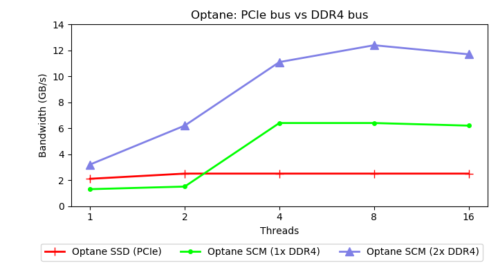
Figure 1 shows the sequential read throughput achievable on Optane storage via

the PCIe bus (Optane SSD) and via the DDR4 bus (Optane SCM). A faster bus yields higher throughput, suggesting that the bus is the bottleneck. Two Optane DIMMs deliver twice the throughput of a single DIMM, suggesting that adding more parallelism within a storage device can deliver higher bandwidth. Even though the faster DDR4 channel removes the limitation of the slower PCIe channel, we can obtain even higher bandwidth if we process data inside the storage device. The next section shows why.
Processing in Memory
Processing-in-memory (PIM) architectures aim to overcome the limitations of memory bandwidth and reduce energy consumption of data movement [4]. There have been many designs that call themselves PIM, ranging from logical gates that work at the level of individual DRAM cells, up to massively parallel, multi-core processor arrays that attach to the memory bus alongside the main CPU. Most of the designs did not make it beyond simulation. We can evaluate a technology with more confidence once it has been implemented in actual hardware, in the form in which it would be used in a real system. Having a viable implementation informs us about what actual shape this technology might take and about its limitations.
That is why, when we learned that a startup called UPMEM [5] has a PIM solution that is on the verge of becoming a commercial offering, we rushed to obtain early access. UPMEM PIM solution is a DDR4-compatible DRAM, it can be used as a drop-in replacement for DDR4 DIMMs. The memory includes small, general purpose processors distributed among the memory modules and tightly coupled with a fixed-sized slice of RAM. Each PIM processor is located in close proximity to its slice of RAM and is attached by a dedicated bus which means both the bus bandwidth and processing capability scale linearly with the amount of available memory. Even though the UPMEM hardware is implemented on DRAM, we believe that the behaviour of SCM is sufficiently close to that of DRAM so we may experiment freely and set expectations about PIM in SCM without depending on simulation or emulation.
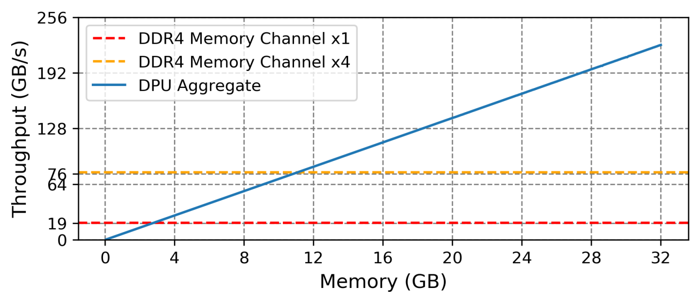
Figure 2 shows the read bandwidth obtainable on UPMEM DRAM as we increase the number of memory chips (and hence the number of PIM processors) used to access data. The flat red line shows the throughput of a DDR channel. While the DDR bandwidth is fixed, limiting how fast the CPU can process data, the PIM hardware can increase the rate of data processing with each additional unit of storage. Certainly computers may have more than one memory channel, but number of channels is limited by the design and number of CPUs in the system. Even a machine equipped with 4 memory channels (the flat yellow line in Figure 2) is quickly outpaced with only 11GB of PIM-enabled SCM.
With 128GB of PIM DRAM and processors at 500MHz, we can obtain up to 2TB/s of read bandwidth which is the target for commercial offering. The experiment in Figure 2 was performed with 266MHz clock rate. This extremely high bandwidth is achievable because PIM processors share very little infrastructure and can operate largely independently. Each PIM processor can read data at the rate of 1GB/s (assuming they are clocked at 500MHz) and with one processor per 64MB chunk of DRAM we have 2048 processors churning on data in parallel.

Although PIM clearly has the potential to tap into the internal parallelism of storage, it also has limitations. In the next section we describe UPMEM PIM architecture in detail and explain why storage-class memory is uniquely positioned to benefit from it despite the limitations.
We believe future PIM designs will likely share many of the features of UPMEM architecture, which was influenced by the constraints of the environment, such as power envelope, physical die size, die process, etc. The fact that PIM has been integrated with DRAM suggests that it will be viable to integrate with SCM, even if not in the same process. At the same time, workloads that make sense to run on SCM, e.g., typical storage workloads that encode/decode, filter and format the data, play well with the limitations of this PIM hardware.

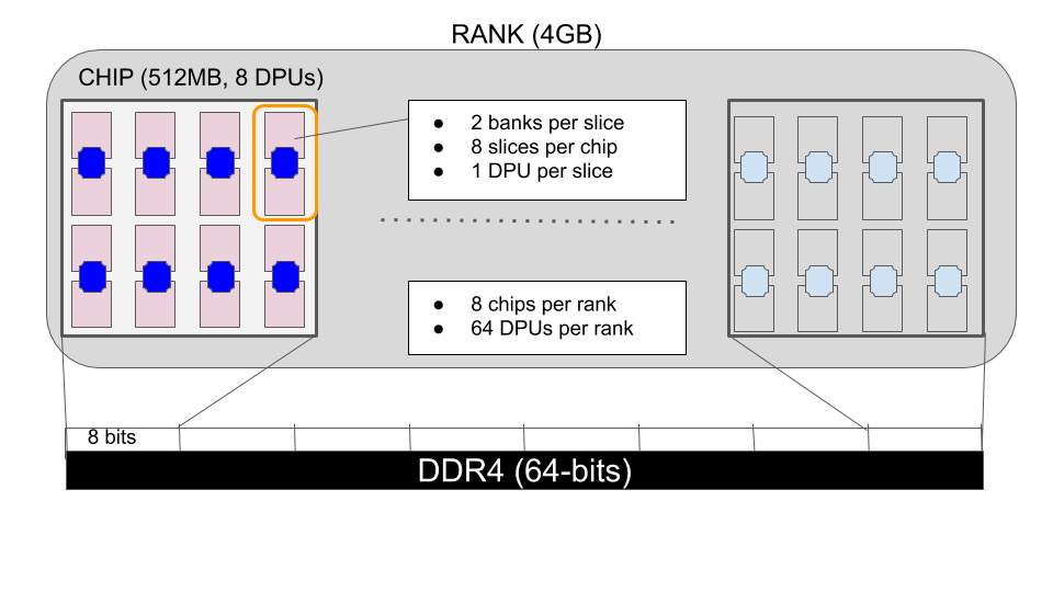
DRAM is organized into ranks, each rank containing eight chips. UPMEM augments DRAM chips by including several DRAM processing units (or DPUs) inside each memory chip. A DPU is a specialized implementation of a general-purpose processor. Each DPU has direct access to a single slice of DRAM over a private bus. The more total DRAM there is, the more DPUs there are. In other words, you get an additional unit of computation with each additional unit of memory - compute scales with storage.
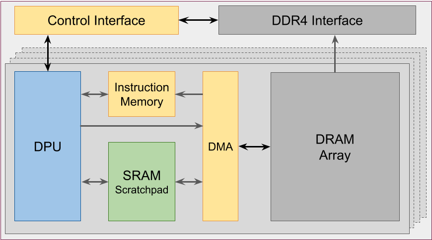
Figure 3 shows a schematic view of a single DPU and its private slice of DRAM. Before a DPU can compute on the data, the data must be copied by a DMA engine from DRAM to a 64KB private SRAM buffer. Each DPU has a large number of hardware threads that can be scheduled for execution, but because it is an interleaved multithreading (IMT) design [6], only one thread can advance at each cycle. The large number of threads helps hide latency while moving data, since several DMA operations can progress concurrently.
The independent operation of the PIM processors is a double-edged sword. Since all of the memory chips are decoupled, all of the DPUs can process data in parallel, completely independent of one another, achieving very high throughput. However, since there is no direct communication channel between DPUs, we must shard data across DPUs and process it in parallel using many threads with little or no communication. Although many algorithms may not have an embarrassingly parallel structure, those used in storage workloads naturally lend themselves to this design. As part of our research we implemented typical algorithms used in storage, such as compression/decompression, parsing, filtering and search on PIM, achieving as much as 10x speedup (with 512 DPUs), but more importantly observing linear improvement in speed with each additional DPU.
Another limitation of PIM is that the capabilities of DPUs are well below that of a common host CPU. Therefore, it is necessary to ensure that the functions they execute are simple enough to be implemented and executed efficiently on these embedded processors. Fortunately, storage workloads that we experimented with fall into this category, executing only a few dozen instructions per byte of processed data (typically in the range of 20-60 instructions per byte), and staying within the capacity of DPUs. For example, compression and decompression workloads utilised the processing pipeline only to 30-60% of full capacity, suggesting that despite its limitation, the processing power of DPUs is sufficient to support this workload.
The final limitation of PIM has to do with how a rank of DRAM chips is attached to the DDR bus [7]. The 64-bit bus delivers 8 bits of data to each chip in the rank. When a host CPU writes a 64-byte cache line to memory, that data is interleaved across DRAM chips at byte granularity. For example, the first byte goes into the first chip, the second byte into the second chip, etc. So when the write is done, the first chip receives bytes at cache-line locations 0, 8, 16, ..., 56. This is a common design in DRAM DIMMs to hide both read and write latency by activating multiple chips simultaneously. This interleaving is transparent to the host since the data written over the bus is read back the same way. In the UPMEM hardware this presents a challenge, because the DPU can only access data in its own chip. When the DPU reads data that has been written to its slice of DRAM, the interleaving causes each DPU to see only every nth byte of the data.

In order to present the DPU with a contiguous dataset, the SDK library must reorder the bytes within the 64-byte cache line before copying them to memory. For example, if we want to write eight bytes contiguously to a slice of memory owned by a single DPU, we would need to place these bytes at locations 0, 8, 16, ... 56 inside the cache line - not the same order that we would need if we wanted contiguous placement for the host CPU. As a result, the host CPU and DPUs cannot share data directly in DRAM, because each needs a different layout. This means that in practice, the host CPU typically copies the data to DPU memory for processing, and then copies it back. In essence, PIM memory is used as an accelerator, rather than native memory organically shared by both types of processors.
Byte interleaving implies that the data stored in PIM-capable memory must be stored in a different format than in conventional DRAM. Although we do not know whether byte interleaving is used in SCM, it presents less of a problem in that context. When persistent storage is PIM-capable, we may offload many operations to the memory and avoid sharing large portions of raw data with the host CPU. By changing the interface, we are free to organize the bulk of the data in a way that is convenient for the SCM, and only re-format the results shared directly with the CPU. Many applications already expect that the data format in storage is different from the format in DRAM, so they already have data conversion functions. This is done for performance, convenience and other reasons. For example, key-value stores use a storage format optimized for compactness (and optionally compressed and encrypted), that is distinct from the in-memory format, optimized for fast search and indexing [8]. Data analytics systems (e.g., Spark, Presto) store data in a portable format (such as JSON, ORC, Parquet) and convert it to the system's internal object representation upon reading the data from storage.
Storage-class memory is giving computer systems a very powerful resource; one that requires a new approach to fully realize its potential. While we will be able to treat SCM like a more traditional storage device for a time, future systems will need to be designed differently to take computing to the next level. PIM's processing capability scales with additional storage, so it is poised to tap into the inherent parallelism of SCM. Although the practical implementation of PIM has certain limitations, storage workloads are a good fit within these constraints due to their highly parallel nature, light computational requirements and specific data formats. That makes PIM and SCM complementary technologies that together may form the basis for future data processing systems.
We would like to thank Rik Farrow, Dick Sites and our anonymous reviewers from HotStorage'20 for their comments and suggestions that help shaped this article. We would also like to thank UPMEM for providing access to their hardware and support.


